Superconducting Architectures and Distributed Interconnects
IBM Watson Lab Develops 80 cm Coherent Interconnect Channel
A team at the IBM Thomas J. Watson Research Center successfully built an 80-centimeter coherent interconnect channel between superconducting quantum chips, achieving a 99% state transfer fidelity and advancing distributed controlled-Z gate (a fundamental two-qubit quantum logic gate, or CZ gate) fidelity to 96.42% ± 0.28%[5]. This milestone maintains high-fidelity inter-chip entanglement over a physical distance of nearly one meter; relative to the current superconducting single-chip SOTA baseline (median on-chip two-qubit gate fidelities of 99.5% to 99.9% in IBM Heron r2 and Google Willow), the current cross-chip CZ gate fidelity of 96.42% corresponds to an equivalent two-qubit error rate (approximately 3.58 × 10⁻²) that remains about an order of magnitude behind the on-chip baseline, yet successfully clears the physical spatial isolation threshold required for modular distributed scaling[5]. Reaching practical deployment still requires resolving cryogenic thermal load dissipation across dilution refrigerators for superconducting microwave links, as well as integrating microwave-to-optical coherent conversion modules[5]. This progress directly benefits full-stack vendors betting on modular multi-chip interconnects and is expected to reshape intra-cryostat chip layout standards within the next 2 to 3 years, reducing single-wafer area yield risks for thousand-qubit-scale superconducting processors[5].
Superconducting 12 ns CZ Gate Approaches Theoretical Limit
Researchers developed a superconducting CZ gate with an operation time of only 12 nanoseconds, approaching the theoretical quantum brachistochrone time limit of 11.6 nanoseconds while achieving intrinsic error suppression down to 2 × 10⁻⁵[6]. Experiments confirmed that even when high-frequency dephasing (random perturbations of quantum coherent states) in the device was increased to seven times existing measured baselines, the gate fidelity remained stable[6]. This metric compresses conventional superconducting two-qubit gate durations (typically 20 to 100 ns) by nearly half, while its theoretical intrinsic error of 2 × 10⁻⁵ effectively pushes fidelity to a 99.998% theoretical ceiling (claimed to surpass published SOTA levels, pending independent verification in multi-qubit arrays)[6]; practical fault-tolerant deployment still lacks empirical verification of parallel-drive crosstalk and leakage to higher energy states within dense multi-carrier-frequency arrays of hundreds of qubits[6]. This breakthrough will reduce the reliance of superconducting quantum chips on frequent calibrations during deep-circuit logical operations, accelerating the maturation of superconducting high-duty-cycle computing architectures[6].
ATS Coupler Achieves Ultra-High 9,922 Noise-Bias Ratio
A research team utilized an Asymmetrically Threaded SQUID (ATS) coupler to construct Kerr-cat bosonic qubit logic gates, achieving a noise-bias ratio of 9,922 (the ratio of phase-flip errors to bit-flip errors) under realistic photon loss rates—improving noise-biasing performance by over 570 times compared to conventional Kerr-cat implementations and attaining a two-qubit gate fidelity of 99.69%[7]. This metric clears the effective threshold for biased-noise fault-tolerant quantum error correction; the 99.69% two-qubit gate fidelity closely approaches the mainstream superconducting production SOTA range (99.5% to 99.9%), and its extreme noise bias allows 2D surface codes to focus primarily on correcting single-axis phase flips, reducing required physical qubit redundancy by several folds[7]; practical deployment, however, remains constrained by residual bit flips induced by multi-photon transition nonlinear dissipation and higher-order microwave channel losses[7]. This progress directly bolsters confidence among hardware startups focused on cat-state bosonic encoding, setting the stage over the next three years for more intense architectural competition between biased-noise error correction and conventional transmon approaches[7].
30 ns Quantum Gate Tolerates 4 MHz Parameter Drift
Researchers engineered a robust quantum gate with a 30-nanosecond gate duration that suppresses coupling error to 6.21 × 10⁻⁷ while tolerating inter-qubit interaction drift of up to 2π × 4 MHz[12]. Compared to conventional superconducting microwave pulse schemes requiring frequent calibration, this gate achieves dedicated error suppression within a standard 30 ns gate window, enabling hardware to passively resist coupling parameter fluctuations caused by environmental noise and thermal drift[12]; measured empirical data on spectral crowding during multi-qubit parallel execution are still lacking[12]. This technique benefits control and measurement system vendors by reducing the proportion of daily calibration time required by superconducting systems, thereby shortening offline maintenance windows for quantum cloud platforms[12].
Neutral-Atom Ecosystem and Systemic Bottlenecks
Assessment of China's Neutral-Atom Ecosystem Reveals System-Level Error-Correction Shortcomings
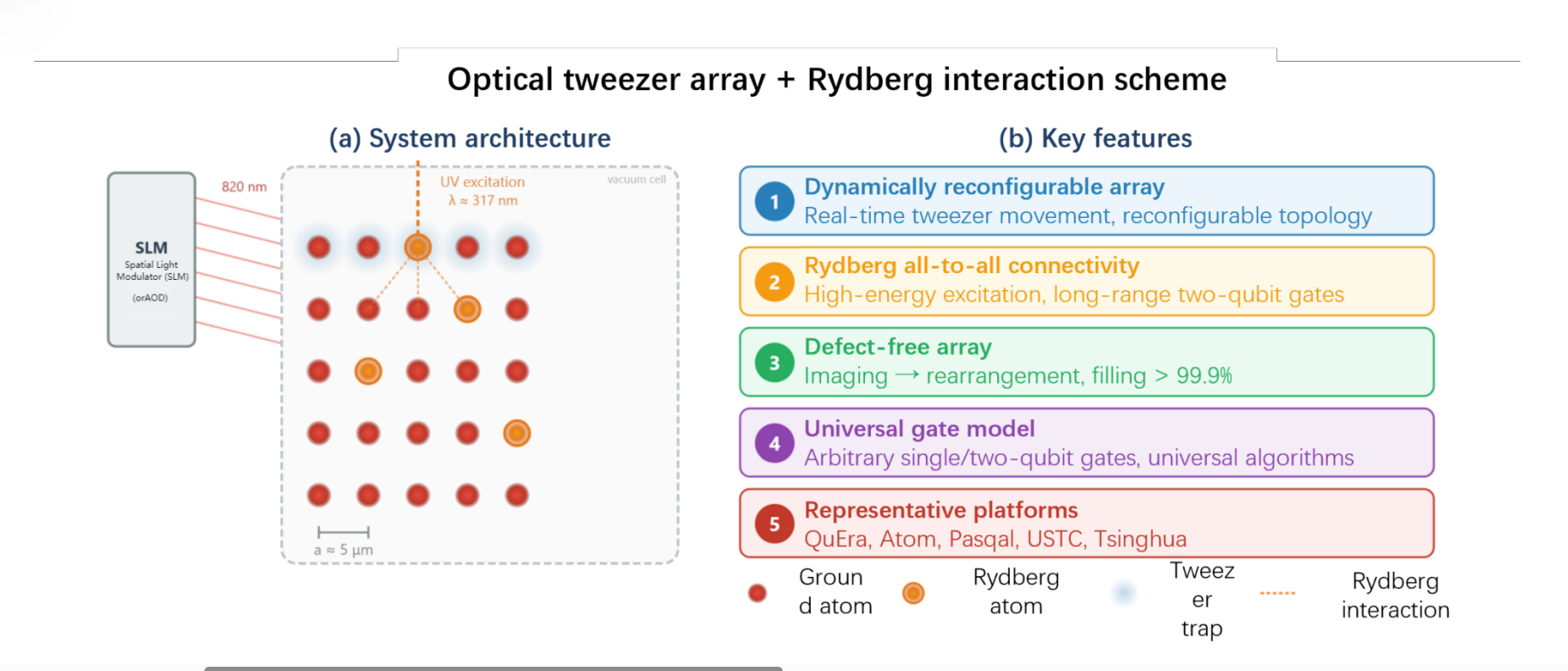
The latest review of China's neutral-atom quantum computing ecosystem indicates that domestic teams have achieved dense hardware milestones in optical tweezer trap array scaling, high-fidelity quantum gates, and commercial full-stack system integration, underpinned by an independent and complete optical and vacuum supply chain; however, they still lag behind European and US teams in system-level quantum error correction and fault-tolerant quantum computing[4]. In terms of physical qubit hardware metrics, domestic multi-thousand-atom trapping capabilities match or exceed Atom Computing's public baseline of 1,180 physical qubits and Harvard University's multi-thousand-atom arrays; yet regarding verified logical qubit metrics, compared to QuEra's demonstration of error-corrected gate operations across 96 logical qubits (based on [[16,6,4]] codes and 448 physical qubits, published in Nature 2026) and Quantinuum's 48 fully error-corrected logical qubits, domestic efforts face a generational gap of 1 to 2 years in real-time error-correction loops and transversal fault-tolerant logic gates[4]. The fundamental hard constraints holding this modality back from practical utility remain the single-cycle repetition rate (currently constrained by a low-frequency bottleneck of 1 to 10 Hz) and the fidelity of non-destructive mid-circuit measurements[4]. This assessment is prompting domestic industry-academia-research alliances to restructure R&D priorities, with capital and research resources expected to accelerate away from mere physical atom count accumulation toward logical qubit encoding and real-time FPGA decoder development over the next 12 months[4].
Solid-State Spins and Color-Center Defects
Germanium-Vacancy Color Center Conversion Efficiency in Diamond Reaches 90%
By introducing germane (GeH₄) during diamond chemical vapor deposition growth, researchers achieved targeted conversion of vacancies into germanium-vacancy (GeV⁻) color center defects within an ultra-thin 10-nanometer layer, reaching a defect conversion efficiency exceeding 90% while maintaining a spin coherence dephasing time (T₂) of over 730 nanoseconds[13]. This technique circumvents the inhomogeneous local lattice strain caused by traditional ion implantation, vaulting conversion efficiency from under 5% in conventional implantation to over 90%, with spin coherence times matching top-tier ion-implanted samples[13]; nevertheless, it still lags three orders of magnitude behind the millisecond-scale coherence baseline of NV centers, and its practical implementation remains reliant on sub-Kelvin cryogenic environments and efficient photon coupling via nanophotonic cavities[13]. This breakthrough provides a high-yield, scalable solid-state color-center material platform for distributed quantum network nodes and on-chip quantum memories, lowering manufacturing barriers for solid-state quantum repeaters[13].
University of Tsukuba Extends Coherence Time to 112 Seconds Using Polarized Spin Bath
A team from the University of Tsukuba in Japan, operating under a 25-Gauss magnetic field, utilized an optically polarized NV⁻ defect spin bath to maintain the spin coherence time of a ¹⁵NV⁻ sensor probe at 112 seconds (a 6.18-fold extension over the 18.1 seconds measured in a conventional P1 defect system of identical density); however, experiments also revealed that this advantage decays as the external magnetic field increases, vanishing entirely at 800 Gauss, where the polarized spin bath underperformed conventional substrates[18]. This experiment elucidates the physical mechanism by which polarized spin baths suppress many-body decoherence at low magnetic fields, advancing coherence lifetimes past the hundred-second threshold[18]; however, this performance reversal at high fields clearly limits the applicability of this method in high-field sensing scenarios such as nuclear magnetic resonance (NMR)[18]. This advance outlines a process optimization path for diamond quantum sensors in low-field, ultra-weak magnetic detection (such as magnetoencephalography and biological weak magnetic sensing), preventing misdirected engineering investments in high-field settings[18].