Superconducting Route
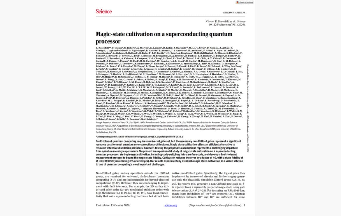
The Google Quantum AI team has completed magic state cultivation (high-purity quantum state preparation technique) benchmarks on its Willow superconducting quantum processor, slashing the preparation error rate of critical T states (non-Pauli higher-order quantum states) by 40x, with experimentally measured error rate upper bounds reaching 1 in 10,000 to 2 in 10,000 (1×10⁻⁴ to 2×10⁻⁴) [7].
- Technical Significance: In current superconducting hardware SOTA benchmarks, Google's Willow previously set an industry record with an error suppression factor Λ ≈ 2.1 using a distance-7 surface code (a 2D lattice quantum error-correcting code). However, non-Clifford gates required for fault-tolerant quantum computing (FTQC) have long been constrained by exponentially ballooning physical qubit overhead. Directing a 40-fold reduction in initial magic state error rates and executing the minimal version of a distillation protocol on real hardware for the first time substantially converges the required error correction rounds and ancilla qubits needed to prepare pure T states. This supports one assumption in Google's previously published projection of "cracking RSA-2048 with fewer than 1 million physical qubits," though the rest of the factory remains untested [7]. Compared to extreme baselines such as commercial trapped-ion all-to-all two-qubit gate fidelity of 99.921% (Quantinuum Helios) and silicon donor fidelity of 99.99% (SQC), superconducting physical two-qubit gate error rates remain in the 0.2% to 0.5% range. Furthermore, this test only covered the minimal version of the distillation protocol; building a fully functional magic state factory still lacks the coordinated control and readout of thousands of physical qubits, and still must overcome coherence time temporal fluctuations of 2x to 3x caused by two-level system (TLS) defects [7].
- Landscape Impact: This reshapes the engineering timeline for fault-tolerant quantum computers breaking classical public-key cryptography, substantially compressing the physical qubit threshold widely estimated by academia from tens of millions down to under one million qubits, compelling global financial, government, and enterprise systems to accelerate post-quantum cryptographic transitions ahead of 2030 [7].
A cat-qubit R&D team has successfully executed core quantum error correction module verification circuits on real superconducting chips comprising 6 and 12 physical qubits [38].
- Technical Significance: Compared to conventional transmon superconducting routes that rely on dual encoding to concurrently correct bit-flips and phase-flips, the cat-qubit approach achieves autonomous exponential suppression of bit-flip errors at the physical level, demonstrating a foundational error correction module [38]. However, advancing toward universal quantum computing still faces shortcomings including high phase-flip error rates and undisclosed CNOT gate fidelities, trailing behind the mainstream superconducting route's hundred-qubit-level engineering integration [38].
- Landscape Impact: Validates the commercial viability of asymmetric noise-biased hardware routes, prompting cloud computing giants to accelerate resource allocation toward bosonic encoding architectures in their superconducting technology roadmaps [38].
Chip fabrication process research has shortened single-die screening and characterization time for atomic-scale quantum chips from 3 hours to 1 hour, boosting single-batch testing throughput by 3x [38].
- Technical Significance: Breaks the industrial cycle-time bottleneck in comprehensive microscopic defect mapping for spin and superconducting chips, providing a rapid screening tool for wafer-level yield management [38].
- Landscape Impact: Significantly reduces the marginal cost per qubit from tape-out to screening for high-density solid-state quantum chips, benefiting downstream system builders in volume packaging and manufacturing [38].
Trapped-Ion Route
(Continuing Coverage: Following previous reports on UK quantum manufacturing funding, highlighting the latest progress in micro-nano packaging yield) The UK National Physical Laboratory (NPL) has officially received a dedicated technology transfer grant of £230,000 from the UK Government Office for Technology Transfer (GOTT), launching a full-scale push on wafer-level packaging processes for micro-nano trapped-ion chips [10].
- Technical Significance: Among trapped-ion SOTA benchmarks, Quantinuum Helios has achieved a commercial all-to-all two-qubit gate fidelity of 99.921% at a scale of 98 qubits. However, trapped-ion architectures are broadly bottlenecked by low assembly yields resulting from complex free-space laser arrays and ultra-high-vacuum (UHV) packaging. NPL’s funding specifically targets volume packaging and electrode wire bonding processes for wafer-scale ion chips, aiming to raise trapped-ion chip process yields to industrial thresholds [10]. Currently, physical ion-shuttling overhead still constrains system cycle repetition rates to the hundred-hertz (Hz) scale, lagging far behind superconducting megahertz (MHz) response times; large-scale scaling still awaits the full maturity of on-chip integrated optical waveguide technology [10].
- Landscape Impact: Drives trapped-ion hardware from national-lab custom fabrication toward standardized foundry manufacturing, accelerating the supply chain autonomy of UK domestic trapped-ion hardware enterprises [10].
Swiss trapped-ion startup ZuriQ has signed a multi-year commercial framework agreement with chip technology vendor Rhonexum, under which Rhonexum will supply custom cryogenic ASICs to ZuriQ to support its next-generation scalable trapped-ion quantum computer roadmap [31].
- Technical Significance: Trapped-ion control and readout previously relied heavily on room-temperature racks and dense coaxial RF cabling. Introducing on-chip 4 Kelvin cryogenic control chips can compress internal interconnect channels by an order of magnitude, fundamentally resolving localized heat dissipation and routing congestion across hundreds of ion trap sites [31].
- Landscape Impact: Marks an inflection point in specialized division of labor across Europe’s trapped-ion supply chain, as full-stack system makers shift to sourcing third-party dedicated cryogenic semiconductor solutions, cutting chip integration R&D cycles by years [31].
Quantum Sensing and Condensed Matter Physics
Fraunhofer Institute for Applied Solid State Physics (IAF) in Germany has developed a diamond quantum sensor based on a laser threshold magnetometer, achieving 100% optical contrast in magnetic field readout for the first time and boosting the sensitivity-to-dynamic-range ratio by up to 590x compared to previous best-in-class benchmarks [4].
- Technical Significance: Previously, optically detected magnetic resonance (ODMR) readout contrast based on diamond nitrogen-vacancy defects (NV centers (luminescent diamond defects)) typically ranged from 5% to 30%, severely limiting photoelectric weak-magnetic detection capabilities in high background light environments. By leveraging optical resonance amplification in a laser gain medium, the team pushed the contrast directly to the 100% physical limit, achieving a generational leap in signal-to-noise ratio (SNR) [4]. However, path-to-portability still requires addressing the power and footprint overhead of pump lasers, as well as uniform doping of luminescent defects across large-area single-crystal diamond [4].
- Landscape Impact: Provides practical sensing probes operating without cryogenic cooling for ultra-sensitive non-invasive magnetoencephalography (MEG) imaging, miniature geomagnetic navigation, and micron-scale internal current short-circuit fault detection in EV battery cells [4].
A research team from Columbia University has published a paper in Science, demonstrating for the first time the localized confinement and spatial trapping of electron waves via quantum interference in a novel layered metallic crystal, Pd₅AlI₂ [5].
- Technical Significance: Completely locks electron wavefunctions through lattice topological destructive interference within a macroscopic 3D metallic network exhibiting high electrical conductivity for the first time, overturning the century-old conventional physical understanding that free electrons in metals must inherently delocalize and diffuse [5].
- Landscape Impact: Establishes a new condensed matter physics foundation for developing zero-dissipation topological quantum interconnect materials and novel correlated-electron switching devices [5].