Oct 14, 2026 – Oct 15 · Daily Brief

Computer Chip Fabrication Yields Quantum Hardware with 0.01% Error Rate

32 items · 12 sourcesPDFThis issue's roundup is free
02Hardware

Hardware Frontiers

Spin Quantum Dots

Researchers operated three spin qubits (encoded using electron spins) simultaneously on a silicon spin quantum chip to execute parallel logic operations, measuring single-qubit gate fidelities exceeding the 99.99% precision threshold[3].

Benchmarked against current state-of-the-art hardware, this result sits at the forefront of the spin modality and provides two technical takeaways: ① Progress achieved: Under the demanding conditions of parallel multi-qubit control, this fidelity matches the previous public record of 99.99% set by Australia's SQC in December 2025 on isolated donor qubits, and suppresses the gate error rate by more than an order of magnitude compared to the 99% median fidelity reported by Diraq and imec on 300 mm wafers (pushing gate error rates below 10⁻⁴ under concurrent three-qubit conditions for the first time), confirming the silicon spin platform's capability to suppress crosstalk during concurrent multi-qubit operation; ② Remaining gaps: On the path toward practical fault tolerance, physical qubit counts for this route remain at the device level (current array sizes generally do not exceed 12 physical qubits, trailing the superconducting Willow chip at 105 qubits and the neutral-atom Atom Computing system at 1,180 qubits), coherence times in isotopically purified silicon (²⁸Si) substrates range from 10 to 100 microseconds, operation counts (the ratio of coherence time to gate duration) remain at only 10² to 10³ (the lowest among the five mainstream hardware modalities), and cryogenic microwave routing fan-out as well as high-fidelity single-shot readout crosstalk still require major breakthroughs.

This milestone provides physical viability proof for industrial players betting on the reuse of mature semiconductor manufacturing lines—such as Intel, TSMC, and Diraq—and is projected to drive commercial foundries to initiate tape-outs and error-correction benchmarking for intermediate-scale spin arrays over the next 24 months.

Superconducting

Google Quantum AI used its 105-physical-qubit "Willow" superconducting processor to conduct experimental explorations into the in situ preparation and purification of "magic states" (resource states essential for universal computation) directly on hardware[11].

Benchmarked against the current state-of-the-art in superconducting hardware: ① Progress achieved: Willow previously established a published industry benchmark with a surface code (a fault-tolerant topological quantum error correction code) error suppression factor of Λ ≈ 2.1; advancing magic state preparation marks a shift in R&D focus from validating error-correction thresholds for Pauli gates to the critical phase of synthesizing non-Clifford gates (logical gates indispensable for universal computation), filling a core gap in realizing a universal fault-tolerant gate set; ② Remaining gaps: Superconducting processors remain limited by energy relaxation times (currently with a median of ~100 microseconds) that exhibit periodic 2- to 3-fold fluctuations induced by two-level system (TLS) material defects, distilling a single high-fidelity logical magic state typically requires an overhead of hundreds of physical qubits, and planar chip area along with cryogenic microwave control wiring density continue to constrain scalable expansion.

This advance solidifies Google's first-mover advantage in fault-tolerant superconducting architectures, putting pressure on IBM (which relies on its 120-qubit Nighthawk roadmap) to accelerate its development of high-complexity circuits and fault-tolerant non-Clifford gate schemes.

Photonics

UK-based ORCA Computing announced the official deployment of its PT-3 photonic quantum computer at a Digital Realty data center in London. Equipped with NVIDIA classical compute acceleration hardware, the system is now open for real-world benchmarking by enterprise users across life sciences, defense, energy, and industrial logistics[29].

Benchmarked against published technical milestones for photonic hardware: ① Progress achieved: The vendor claims the unit is the first photonic quantum system engineered specifically for commercial quantum utility/advantage (computational speedup over classical supercomputers), utilizing time-multiplexed fiber delay loops and a classical-quantum heterogeneous co-processing architecture; however, these metrics currently reflect vendor white papers and commercial announcements, pending independent third-party verification; ② Remaining gaps: Compared against published benchmarks for photonic hardware (PsiQuantum's measured two-qubit fusion fidelity of 99.22% and superconducting single-photon detection efficiencies of ≥95%), the PT-3 has not disclosed an end-to-end optical loss budget or un-postselected fidelities; its non-deterministic single-photon sources based on fiber loops and electro-optic switches suffer cumulative optical loss upon scaling, leaving a substantial gap before universal fault-tolerant computation can be reached.

As Europe's first rack-scale photonic quantum hardware deployment inside a commercial colocation data center, this system will compete against quantum annealers and superconducting cloud platforms over the next 1–2 years for enterprise hybrid compute budgets.

Quantum Annealing

At the 2026 Digital Innovation Forum, D-Wave Systems announced that its next-generation Advantage2 quantum annealing computer (which leverages quantum effects to find optimal solutions) has arrived at Villa Saporiti in Como, Lombardy, Italy, for installation[23].

Compared with its predecessor, the Advantage2 system improves superconducting qubit interconnect connectivity and physical coherence times, reducing freeze-out errors when solving combinatorial optimization problems. While the quantum annealing architecture lacks gate-model universal logical error correction, it provides specialized solver performance on constrained Quadratic Unconstrained Binary Optimization (QUBO) mathematical models.

This represents a major on-premises hardware delivery for D-Wave in continental Europe, strengthening its industrial adoption across Southern Europe and reinforcing its commercial baseline for securing industrial optimization contracts ahead of gate-model commercial maturity.

03Algorithms

Algorithms & Software

Rare-Event Simulation Algorithms

On October 15, 2026, the international physics journal Quantum published a paper in which researchers developed a "rare-event simulation" (efficient computation of vanishingly small probability events) numerical algorithm targeting logical error rates in quantum error correction circuits[10].

At low physical component failure rates, conventional Monte Carlo methods (numerical calculations based on random sampling) face severe computational bottlenecks due to the massive sample sizes required. By applying importance sampling techniques, this algorithm reduces the classical simulation runtime for logical failure rates by over 90% when physical error rates drop below 10⁻⁴, making it possible for the first time to evaluate the true decay curves of larger-scale logical circuits under ultra-low-noise regimes on standard computing nodes[10].

This algorithm will provide computational tool support for teams such as Google and Quantinuum in designing compact surface codes and low-density parity-check (LDPC) decoders, shortening error-correcting code optimization cycles.

Photonic Chip EDA Simulation

Integrated photonics simulation software startup EMode Photonix completed a $1 million pre-seed funding round led by Ground State Ventures, with participation from Harlow Capital Management[24].

The team focuses on developing foundational EDA simulation tools for photonic quantum computing chips, providing high-precision modeling of microring resonators, beam splitters, and nonlinear waveguide losses. This bridges the software tooling gap in conventional microelectronics design platforms, which cannot accurately simulate on-chip single-photon interference and quantum optical state evolution[24].

Securing early-stage venture backing for specialized software toolchains will help photonic quantum hardware teams reduce tape-out trial-and-error costs for photonic integrated circuits (PICs) and compress engineering lead times from layout design to wafer delivery.

Software Abstraction Layer Research

A European academic consortium established a two-year postdoctoral R&D position dedicated to quantum software abstraction layers, focusing on semantic abstraction standards for high-level instruction sets decoupled from underlying physical gate pulses[9].

The project aims to establish a universal intermediate representation (IR) spanning heterogeneous hardware architectures—including superconducting, trapped-ion, and spin platforms—accelerating the evolution of the quantum software stack toward layered decoupling[9].

Academia's accelerated push to build middleware analogous to classical operating systems will lower cross-platform deployment barriers for high-level quantum algorithm developers.

04Industry

Industry & Ecosystem

Cybersecurity & Semiconductors

Nasdaq-listed semiconductor and security firm SEALSQ released unaudited financial results for the first nine months of 2026, reporting a 65% year-over-year revenue increase[21], alongside an announcement that it will showcase its complete suite of post-quantum security chips at Electronica Munich from November 10–13, 2026[26].

The 65% revenue growth confirms that post-quantum cryptography (algorithms designed to resist quantum attacks) is transitioning from regulatory compliance discussions into a hardware procurement realization phase, with its hardware security modules (physical secure chips protecting cryptographic keys) and root-of-trust products already generating commercial deliveries for critical IoT and automotive terminals[21][26].

This offers a clear earnings signal for the cybersecurity sector, compelling traditional microcontroller manufacturers to accelerate the integration of post-quantum cryptographic engines into production silicon.

Blockchain Standards Consortium

Leaders from nine global blockchain organizations co-founded the "Quantum Alliance" on October 15, 2026, to jointly establish evaluation criteria for quantum-resistant cryptographic algorithms and cross-network migration specifications for distributed ledgers[22].

The alliance will formulate benchmarks and criteria for evaluating distributed networks against quantum retro-analysis and attack, driving signature algorithms to transition from legacy Elliptic Curve Digital Signature Algorithms (traditional public-key cryptographic signatures) toward lattice-based cryptographic frameworks[22].

Unified specifications will pressure major public blockchains to accelerate protocol-level hard forks over the next 1–3 years, mitigating future vulnerability exposure for trillions of dollars in decentralized digital assets.

University-Industry R&D Centers

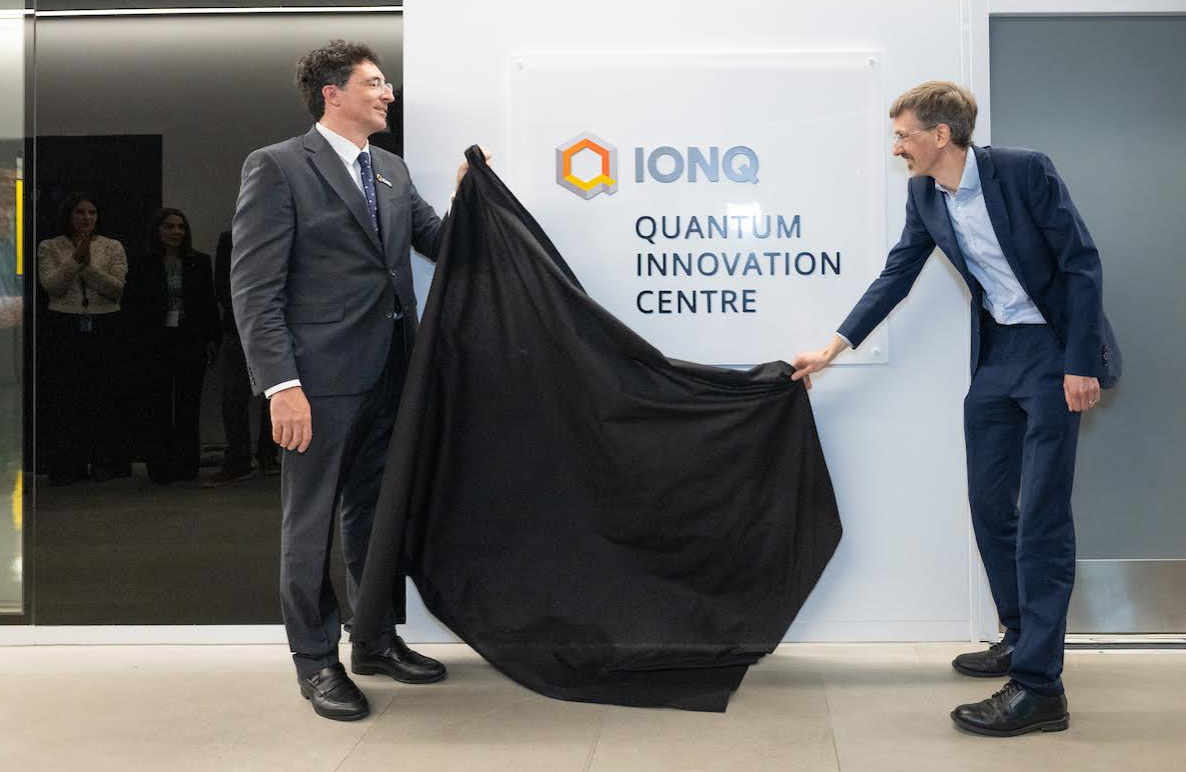
Full-stack trapped-ion quantum computing company IonQ and the University of Cambridge officially opened their first university-embedded Quantum Innovation Centre at the Ray Dolby Centre within Cavendish Laboratory[20].

Following its previously announced $2.0 billion private placement financing, IonQ has established an R&D entity directly in the cradle of premier UK academia, deeply interfacing with local condensed matter physics resources and cultivating full-stack hardware engineering talent[20].

This move intensifies the integration of European academic ecosystems and government quantum initiatives by multinational full-stack giants, mounting competitive pressure on local European hardware startups.

Shift in Government and Institutional Funding

Funding mechanisms from global governments and financial institutions for quantum finance are undergoing a strategic pivot, with capital allocations steering decisively toward two engineering deployment tracks: portfolio risk calculation and post-quantum cryptographic network migration[2].

Sovereign wealth funds and financial institutions are concentrating capital into dedicated algorithm benchmarks that deliver verifiable computational speedups and infrastructure security defense[2].

Quantum technology budgets across global systemically important banks (G-SIBs) are steadily transitioning into recurring annual risk management and IT infrastructure expenditures, accelerating procurement conversions for specialized software and hardware.

Software-Defined Secure Networks

Software-defined networking provider ZeroTier released Release Candidate 3 (RC3) of its ZeroTier Quantum platform, marking the final step toward full production deployment of end-to-end post-quantum virtual private networks[27].

This release finalizes the engineering integration of post-quantum key encapsulation mechanisms with existing network protocol stacks, demonstrating that VPNs can achieve post-quantum hardening for underlying data transit through software-only upgrades[27].

As a result, the marginal cost for enterprise users to deploy post-quantum communications has dropped, facilitating a smooth transition of legacy network traffic to post-quantum protocols.

European Skills Training Alliance

Nordita (Nordic Institute for Theoretical Physics) in Stockholm announced Sweden's official entry into the European Quantum Skills Academy alliance, establishing a standardized quantum engineering talent training system across Europe[19].

The initiative aims to build unified technical training and professional qualification standards to alleviate the shortage of interdisciplinary, high-caliber technical talent in hardware experimental platforms and systems software engineering[19].

05Other

Academic Frontiers

Physics of Solid-State Spin Defects

Using high-precision quantum many-body theoretical models, researchers elucidated at the atomic scale the microscopic dynamical pathways through which optical excitations in spin defects (atomic defects used for emission in crystal lattices) within diamond and silicon carbide dissipate energy via phonon channels[4].

The study quantitatively reproduces non-radiative decay processes mediated by electron-phonon coupling, providing theoretical data to unravel how localized lattice vibrations limit coherence times in solid-state optically active defects[4].

These findings supply structural tuning guidelines for designing room-temperature, long-coherence quantum sensors and telecom-band solid-state quantum memory probes, helping guide semiconductor defect engineering.

Quantum Sensing for Gravitational Measurements

Theoretical physicists proposed a design using ultracold atom-interferometry quantum sensors to directly measure the Earth's rotation-induced "frame-dragging effect" (the dragging of spacetime by a rotating mass) within a terrestrial laboratory[5].

By exploiting long-interrogation-time atomic matter-wave interferometry, this design pushes the sensitivity for detecting spacetime curvature and weak inertial frame rotations to the quantum limit, removing the historical reliance on high-orbit gravitational satellites[5].

This theoretical framework will propel the development of high-precision atomic gyroscopes and gravity gradiometers, providing technical references for passive inertial navigation and precision geodesy.

Room-Temperature Quantum Memory

The Qu-MEM room-temperature quantum memory (a medium for controlled storage of quantum states), developed by Stony Brook University and commercialized by Qunnect, was selected for TIME magazine's Best Inventions of 2026 list (Experimental category)[18].

Operating via electromagnetically induced transparency (EIT) in a warm atomic vapor cell, the rack-mountable device achieves low-noise storage and retrieval of single-photon states across the telecom C-band (the primary transmission band for fiber communications) at room temperature, eliminating reliance on ultra-low-temperature dilution refrigerators[18].

The unit reduces power consumption and deployment complexity for quantum repeater nodes, offering a field-ready hardware candidate for metropolitan quantum testbed networks.

Fundamental Limits in Quantum Thermodynamics

On October 15, 2026, Physics World reported on a fundamental quantum bound derived by physicists governing the timescale required for an open quantum many-body system to equilibrate (reach internal temperature uniformity)[6].

The theoretical proof shows that the rate at which a microscopic physical system reaches thermal equilibrium through heat exchange with an external bath has an absolute lower bound determined by the Planck scale, setting the fastest physical limits on dissipation and cooling in open quantum systems[6].

This bound provides fundamental theoretical limits for the thermal design of ultra-low-temperature cryocooler cold plates and heat sinks in superconducting and semiconductor quantum chips, guiding thermal impedance optimization for cryogenic interconnects.

European Industry Investment Initiative

Ignacio Cirac, recipient of the Institute of Physics Newton Medal, issued an open appeal calling on European governments and private capital to significantly boost direct investment into the domestic quantum hardware supply chain[7].

Cirac urged Europe to establish larger dedicated sovereign investment funds to prevent the domestic supply chain from offshoring during the pivotal transition from laboratory proof-of-concept to chip-scale industrial manufacturing[7].

Resource Exploration & Specialized Navigation Deployments

Dirac Labs officially joined the Wisconsin Security Research Consortium to develop spoof-resistant autonomous maritime navigation systems[25]; meanwhile, Felgan Ventures published industry research noting that against the backdrop of an International Energy Agency forecast predicting an ~25% global copper supply deficit by 2035, quantum gravimeters (instruments measuring minute variations in gravitational fields) are accelerating their replacement of traditional airborne magnetic and electrical geophysical prospecting methods in deep geological exploration[28].

Quantum gravimetry directly utilizes matter-wave interferometry to detect subterranean density anomalies, delivering superior penetration depth and interference immunity compared with conventional electromagnetic induction equipment[28].

Quantum precision sensing is becoming the first sector to establish positive cash-flow business models in resource exploration and dual-use, satellite-denied navigation, emerging as a specialized market segment capable of commercial self-sufficiency without waiting for universal fault-tolerant logical error correction[25][28].


06Other

Key Takeaways Today

  1. Semiconductor Foundry Reuse Route Secures Pivotal Physical Evidence[3]: The silicon spin platform surpassed a 99.99% gate fidelity under parallel three-qubit operation, overcoming the parallel control crosstalk bottleneck that has long troubled semiconductor spin chips and confirming that mature microelectronics processes can support the fabrication of quantum hardware with ultra-low error rates. Chip manufacturing giants like TSMC and Intel, along with their investors, will accelerate their evaluations of volume manufacturing viability for spin quantum processors. The key metric to monitor next will be comprehensive distribution benchmark data across all qubit pairs on 300 mm wafer spin arrays in 2027.
  2. Crypto Assets and Critical Network Infrastructure Face a Concrete Post-Quantum Migration Window[21][22][27]: The formation of the Quantum Alliance by nine leading blockchain organizations to unify post-quantum standards, combined with ZeroTier's RC3 release and SEALSQ's 65% year-over-year revenue growth in the first three quarters, indicates that post-quantum cryptography has moved past proof-of-concept into the phase of protocol hard forks and scaled hardware security chip procurement. The defensive window for securing trillions of dollars in on-chain assets and multinational enterprise data is narrowing. The next milestones to track include testnet progress for post-quantum signature improvement proposals on major public chains like Ethereum, as well as mandatory chip-replacement mandates for government infrastructure following the release of international standards.
  3. R&D Cycles for Fault-Tolerant Error Correction Algorithms and Underlying Design Tools Compress[10][11][24]: A new rare-event simulation framework slashes classical simulation runtime for logical error rates under ultra-low physical error conditions by over 90%. Coupled with experimental progress in in situ magic state preparation on Google's Willow chip and venture backing for a photonic EDA simulation startup, theoretical and tooling hurdles facing fault-tolerant quantum computing are steadily diminishing. Chip design iteration cycles for hardware teams are poised to shorten. The next milestone to watch will be Google's disclosure of single logical magic state distillation fidelities and physical resource overhead ratios on the Willow architecture.
  4. Quantum Precision Sensing Establishes Positive Cash Flow First in Resource Exploration and Specialized Navigation[18][25][28]: Stony Brook's room-temperature quantum memory being named to TIME's annual inventions list, coupled with the launch of the maritime spoof-resistant navigation consortium and surging demand for gravity-based deep copper exploration, demonstrates how quantum sensing and networking hardware can generate commercial value leveraging currently viable technology—without waiting for the maturation of millions of universal fault-tolerant logical qubits. Investment targets tied to geophysical prospecting and autonomous vehicle navigation are entering an operational inflection point. The next milestone to watch is the field reliability and continuous operating stability metrics of vehicle- and vessel-mounted mobile quantum gravimeters in rugged prospecting environments.
07Other

Editor's Notes

A strategic bifurcation across the quantum technology landscape is becoming increasingly evident. On one side, the universal quantum computing camp—spearheaded by silicon spin and superconducting circuits—is navigating deep technical waters to conquer unforgiving physical metrics. Whether suppressing microwave crosstalk during concurrent multi-qubit operations in silicon or exploring hardware-native magic state distillation for universal gate sets in superconducting circuits, the underlying imperative remains pushing physical error rates past the fault-tolerance threshold. This path demands towering technical barriers, multi-year R&D timelines, and massive capital expenditures. Yet, silicon spin achieving a fidelity above 99.99% compels the market to reassess the strategic leverage of existing semiconductor manufacturing infrastructure; long-term universal hardware competitiveness will hinge not only on leading physical metrics, but also on process compatibility with mature commercial foundries.

Simultaneously, non-universal commercial monetization is accelerating. Sustained revenue growth in post-quantum encryption silicon, the creation of cross-chain blockchain standards, and the deployment of quantum gravimeters and room-temperature memories across mineral exploration and maritime navigation all show that commercial capital is pragmatically flowing toward near-term products offering unambiguous defense value or quantum-advantaged sensing precision. Investment capital is cleaving into two strategies: one focused on capturing near-term positive cash flows driven by cryptographic compliance and specialized sensing contracts, and another continuing to back foundational milestones along the long-term roadmap toward fault-tolerant universal quantum computing. This divergence is steering the broader quantum sector away from early conceptual posturing and into an era of rigorous engineering execution.