Superconducting Chips and Fabrication Processes
IBM and Rutgers University, using a 100-superconducting-qubit processor, successfully drove and locked the evolution of a many-body quantum system from a chaotic, divergent state into a controlled, stationary dynamic regime by executing thousands of mid-circuit resets (measure-and-reset operations during computation)[12]. [Benchmark vs. Superconducting SOTA Baseline] This experiment demonstrates the capability of non-unitary (trace-decreasing / non-probability-preserving) dissipative operations to suppress phase-space divergence, but its underlying physical mechanism is by no means quantum error correction; the current gold standard in superconducting error correction remains the below-threshold surface code demonstrated by Google's Willow system (an error suppression factor Λ ≈ 2.1 at code distance d=7), whereas this experiment completely lacks syndrome measurements (measuring ancilla qubits to detect errors) and a logical qubit error-correction loop[12]. While this technique provides a new approach for noisy quantum hardware to simulate non-equilibrium condensed-matter physics, it cannot replace error-correcting codes on the roadmap toward general-purpose fault-tolerant quantum computing and is expected to remain largely confined to academic physics research over the next 3 to 5 years[12].
The Superconducting Quantum Materials and Systems Center (SQMS), led by the US Fermi National Accelerator Laboratory (Fermilab), completed a multiscale microstructural materials characterization study that precisely correlates microscopic grain-boundary defects and microfabrication processing features in superconducting 3D cavities and transmon qubits (charge-noise-insensitive superconducting qubits) with device decoherence fluctuations[2]. [Benchmark vs. Superconducting SOTA Baseline] Energy relaxation times (excited-state decay lifetimes) (T₁) of leading superconducting devices typically span 100 to 500 microseconds (e.g., Google's Willow reaches ~100 µs), but the industry broadly faces 2- to 3-fold temporal random fluctuations induced by two-level systems (TLS, microscopic defect absorbers in materials); by elucidating the microscopic sources of high-frequency loss at interface oxide layers, this study provides a clear process-improvement roadmap to break through the 500-microsecond coherence bottleneck[2]. These fabrication insights will directly influence thin-film growth and cleanroom specifications for full-stack manufacturers such as IBM and IQM, and are projected to drive updates to upstream high-purity target material and wafer processing standards in superconducting hardware within 2 years[2].
Trapped Ions and Hybrid Architectures
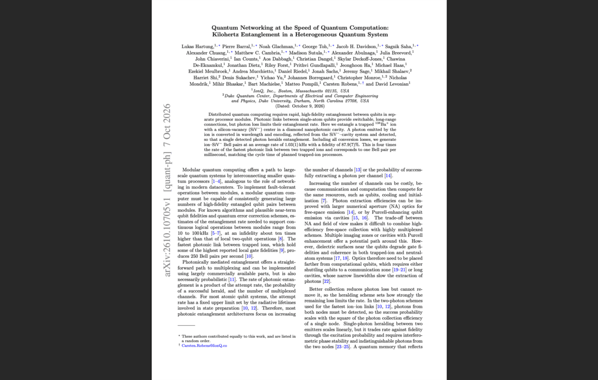
Following reports from October 10, 2026 (Beijing Time), a third-party technical evaluation further analyzed empirical data from trapped-ion vendor IonQ's optical link connecting a single barium ion to a diamond silicon-vacancy (SiV, an optically active point defect in diamond) color-center memory, which achieved an entanglement distribution rate of 1,000 per second with an entanglement fidelity (overlap between the actual and ideal states) of 88%[11]. [Benchmark vs. Trapped-Ion and Interconnect SOTA Baseline] Although 1,000 per second is 4 times faster than the previous record for photonic interconnects between trapped ions, the 88% fidelity lags far behind the trapped-ion two-qubit gate SOTA (IonQ's own EQC prototype at 99.99% and Quantinuum's commercial all-to-all qubit pairs at 99.921%), as well as the photonic interconnect SOTA (PsiQuantum's 99.72% fidelity over a 42-meter fiber link); more crucially, IonQ's own academic publications argue that inter-module entanglement rates required to build a distributed fault-tolerant computing network range between 10,000 and 100,000 per second, meaning current measured hardware performance trails theoretical thresholds by a factor of 10 to 100[11]. This gap indicates that fiber-interconnected distributed trapped-ion computing clusters cannot replace single-chip scaling in the near term, and a modular multi-chip tiling roadmap will require at least 5 to 7 more years of dedicated optical engineering breakthroughs[11].
An international research team utilized a trapped-ion quantum simulator to successfully simulate the non-perturbative dynamical evolution of gluon string breaking (the deconfinement process of quarks) in high-energy physics[10]. By leveraging the all-to-all Coulomb interactions of an ion chain to construct gauge field models, the experiment verified the feasibility of real-time dynamical reconstruction of extreme high-energy physics phenomena on quantum hardware[10]. This achievement accelerates the penetration of quantum simulation into premier particle physics hubs such as CERN, with expectations to become a supplementary verification tool for strongly correlated particle simulations within 3 to 5 years[10].
Photonic Quantum and Communication Links
The European Space Agency (ESA) officially confirmed the achievement of its targeted space communication milestones, reaching a generation rate of polarization-entangled photon pairs (polarization-correlated photon pairs) exceeding the 1 GHz (1 billion pairs per second) technical threshold in the 1560 nm telecom band[21]. [Benchmark vs. Photonic SOTA Baseline] A 1 GHz generation rate boosts transmitter throughput for satellite-to-ground quantum communications by nearly 10-fold compared to previous hundred-megahertz experimental sources, fully matching the requirements of high-bandwidth quantum key distribution (QKD, distributing keys via quantum states) and distributed quantum compute clustering; on the receiving end, however, overall end-to-end system loss remains constrained by atmospheric attenuation and the single-photon detection efficiency of superconducting nanowire single-photon detectors (SNSPDs, baseline requirement ≥95%)[21]. By clearing the engineering hurdle on the transmitter side for high-speed secure space communications, this technology will directly support the deployment of Europe's next-generation quantum satellite constellation, with pan-European orbital key distribution service validation expected around 2028[21].
Dutch quantum research institute QuTech completed the full relocation and delivery of a key quantum hardware experimental testbed to the Karlsruhe Institute of Technology (KIT) laboratories in Germany[22]. This cross-border transfer signals that European research collaboration in topological and superconducting hybrid quantum devices has transitioned from concept to transnational equipment sharing, shortening verification cycles for novel devices across Germany and the Netherlands[22].
Neutral Atoms and Topological States of Matter
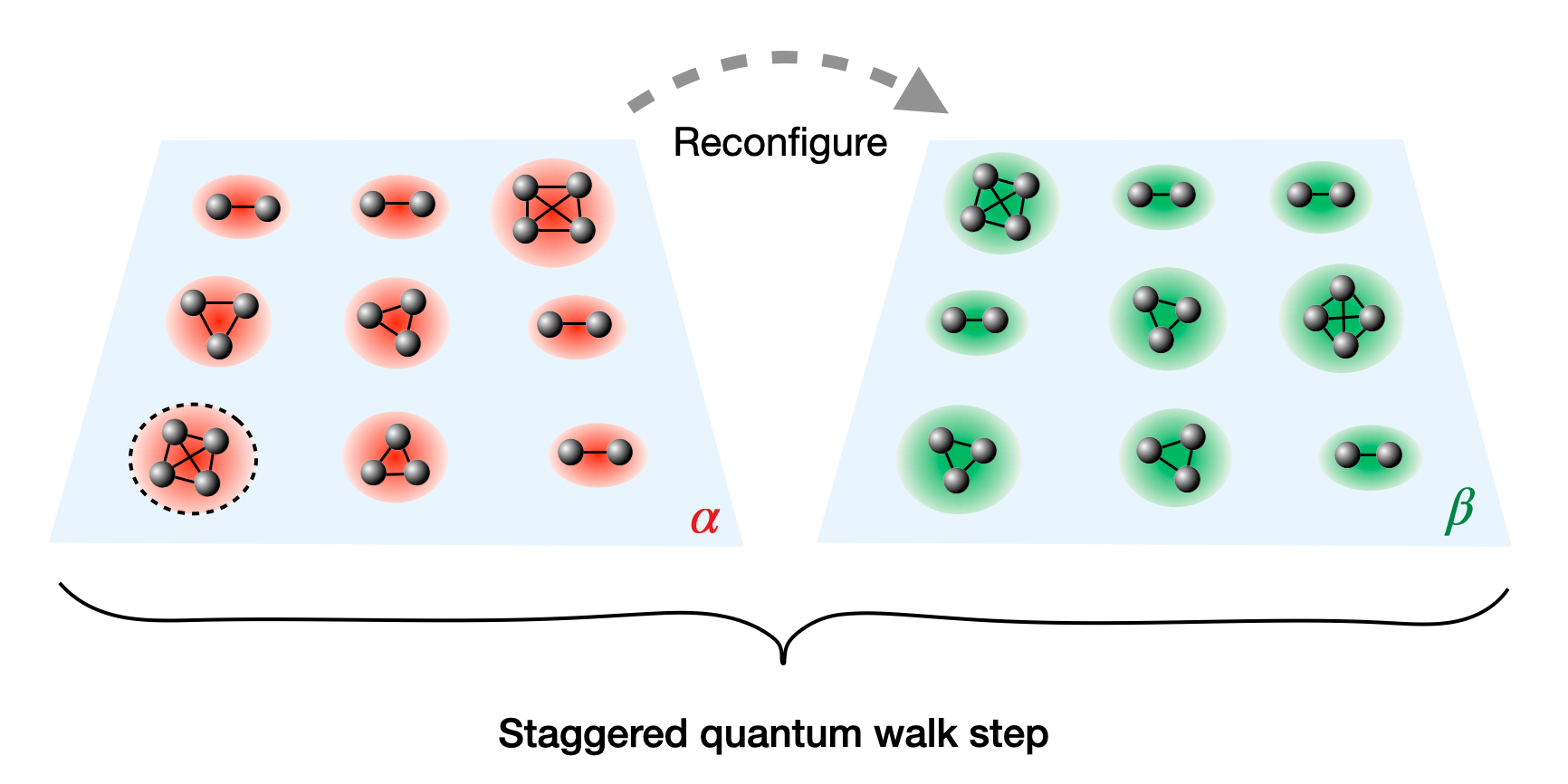
Researchers published findings in Quantum proposing a theoretical implementation for simulating continuous-time quantum walks (CTQW, the spreading of quantum states across a network) on arbitrary topological spatial graph architectures using optical tweezer arrays of precisely arranged Rydberg atoms (atoms with valence electrons excited to high principal quantum numbers)[19]. [Benchmark vs. Neutral-Atom SOTA Baseline] This scheme circumvents the geometric dimensionality limitations of traditional static optical lattices by exploiting the dynamic site-rearrangement capabilities of neutral atoms to construct non-Euclidean spatial topologies; however, constrained by the 1 to 10 Hz cycle repetition rate typical of neutral-atom platforms, simulation runtimes for larger-scale graphs remain prolonged[19]. This advance offers a brand-new quantum topological evolution testing framework for graph-theory challenges such as community detection in social networks and routing optimization in transportation logistics[19].
Materials scientists developed a novel "carpet-mode" surface epitaxial growth technique, successfully fabricating large-area, uniformly thick thin films of two-dimensional topological insulators (materials that are insulating in the bulk but conductive along their edges)[6]. Featuring dissipationless, unidirectional edge spin conduction alongside bulk insulation, this material provides a high-quality physical substrate for engineering highly stable Majorana fermion topological qubits, and is projected to help the topological hardware route overcome material uniformity challenges over the next 3 to 5 years[6].
Physicists fabricated scanning tunneling microscopy (STM) tips from layered topological materials to directly capture, for the first time at atomic spatial resolution, the electronic state signatures of two-dimensional altermagnetism (a spin-split magnetic order with zero net magnetization)[8]. This technique fills an instrumentation void in atomic-scale local spin probing, opening up a new observational toolkit for developing novel spin-based quantum memories and ultra-low-power, dissipationless spintronic devices[8].